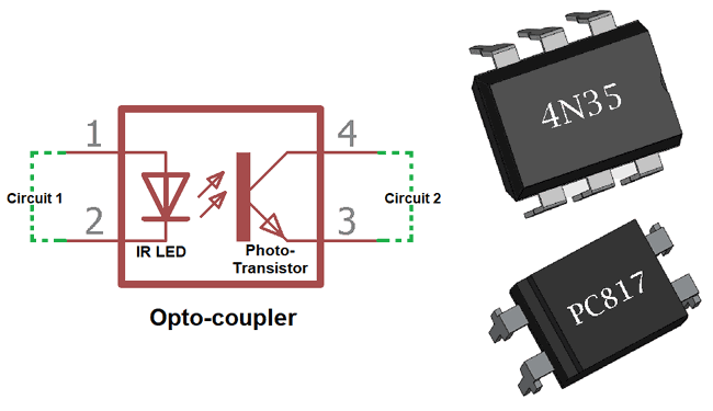
Optoisolators are a component that is used as a component of I / O control for equipment that operates with DC or AC voltage. An optocoupler consists of GaAs LEDs and NPN phototransistor made of silicon.

In Figure a. optoisolator gets a TTL input in the form of a box signal so that the output is also a box signal but the voltage level changes to 0- + 24 volts.
In Figure b optoisolator is used in the modulated input with the voltage Vin isolated with Vout modulation with peak voltage + 12V.
The most important factor in I / O interfaces, especially for loads that use AC voltage, isolation is the most important and must be considered in the design. The digital system uses a + 5volt voltage level while the load uses a 220VAC voltage. This voltage difference is enough to cause the digital control system, PC for example, to be damaged if the port on this computer receives an impact voltage from a 220VAC load.

As shown in the schematic diagram above, the optoisolator gets a voltage of 115VAC but the current is passed only 8mA and the current of this magnitude is enough to make the phototransistor active and the logic received by the inverter becomes ‘low’. With this circuit, we get periodic pulses with the same frequency as the 50Hz PLN voltage but in the form of a box pulse. With the pulse on Pulse Out, it can be ascertained that there is still a voltage on the PLN network while if there is no pulse again, it can be ascertained that the PLN network voltage is 0 VAC.
If a high switching speed is needed, the optoisolator must be configured so that the photodiode is used as shown:

Another way to isolate between high voltage circuits and low voltage circuits is to use a relay. The disadvantage of a relay is the price of a relay with a large current capacity is quite expensive, the size of the relay dimension is large so that the PCB used is also greater, causing noise signals, and the response is slow. While using an optocoupler, the size is small so the PCB size becomes smaller and in the end the equipment becomes smaller too, the response speed is faster