Table of Contents
- Circuit Diagram
- Circuit Diagram using Breadboards
- Electronic Diagram
- How schematic diagram can be defined in general?
- Advantages of using the Schematic diagram
- Electronic Schematic Drawing Symbology
- Electronic symbols of Solid state devices, Switches, Fuses, Meter
- Electronic schematics
- Reading electronic prints or schematics
- Block Diagram
- Block Drawing Symbology
- Connection Diagrams
- Rules for drawing Schematic
Electronic components come in a wide variety of sorts, making up electronic products. These elements can all be pictured or symbolically represented.
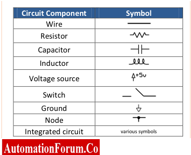
Circuit Diagram
- A circuit diagram is the first element an engineer’s create before designing a circuit.
- A circuit diagram is comparable to a user guide or road map for the circuit.
- The identical circuit can be built by others by having them read the circuit schematic.
- To indicate where various circuit components are located, engineers employ specialised symbols.
- The most prevalent circuit components and their symbols are listed in below table
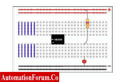
Circuit Diagram using Breadboards
- Breadboards are used in beginning to design, build and test a new circuit
- A breadboard does not require soldering it uses insulated wire.
- A circuit’s initial design is rarely its final design, it is first created using a tool that allows the engineer to easily move components around as needed
Electronic Diagram
- Electronic schematics are the most complex kind of electronic drawings.
- They display every component in a circuit along with its technical details (such as ratings) and wiring diagram.
- A block diagram is the most basic type of drawing.
What is the main purpose of a schematic?
- Schematic refers to a model, plan, or outline of circuit diagram.
- A simple, understandable graphical representation of a plan or model is what a schematic diagram is.
- Simple lines and symbols are used in schematics to convey details like what, how, and where.
How schematic diagram can be defined in general?
- Schematic diagram is similar to blueprints of house.
- Schematic diagrams, also referred to as circuit diagrams or fundamental diagrams, are essentially blueprints that depict the connections between various processes or components.
- When laying out the connections in an electrical circuit, they are very crucial for electrical engineers.
- These schematic diagrams use lines to represent wires and circles to represent power supplies to visually represent the components of a circuit.
- This design makes it simple to decide how to layout a circuit and to pass plans to other team members for straightforward implementation.
Advantages of using the Schematic diagram
Identify issues quickly: By visualzing the functional relationships in an electrical circuit, you can quickly identify any potential issues before they materialize into actual ones.
Extensively customizable: You may easily edit your diagram with a few clicks. Re-sharing is simple, so your team can easily keep in sync with updated documentation.
Electronic Schematic Drawing Symbology
- Electronic schematics offer the most information and depth about a circuit of any kind of electronic layout.
- Every electronic component in a given circuit will be represented, and in the majority of situations, its rating or other pertinent component information will be included.
- The degree of information required to diagnose electronic circuits is provided by this kind of depiction.
- In a schematic layout of an electrical or electronic circuit, an electronic symbol is a pictogram that is used to represent various electrical and electronic components or functions, such as cables, batteries, resistors, and transistors.
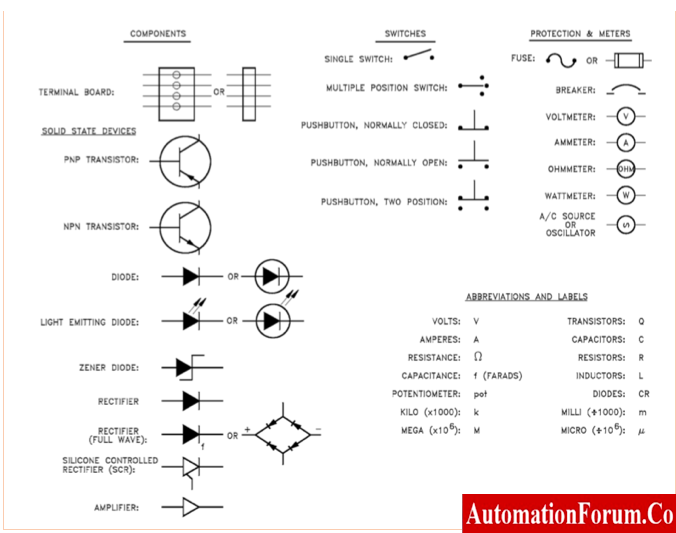
Passive Component and Meters
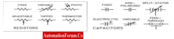
Resistors
- Basic circuit components and symbols of schematics show resistors as zig-zag lines with two terminals.
- Instead of squiggles, international symbol schematics may use a featureless rectangle.
Potentiometers
- Variable and potentiometer resistors have arrows.
- Since the variable resistor is two-terminal, the arrow is diagonally across the middle.
- The arrow is the potentiometer’s third terminal (the wiper).
Capacitors
- Two capacitor symbols are common. Symbols for polarised (usually electrolytic or tantalum) and non-polarized capacitors are shown.
- Each plate has two perpendicular terminals.
- Polarized capacitors have one curved plate.
- The capacitor’s cathode—the curved plate—should be lower in voltage than the anode pin.
- The polarised capacitor symbol’s positive pin needs a plus sign.
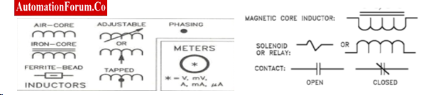
Inductors
- Typically, inductors are shown as loopy coils or as a collection of curved bumps.
- An inductor may simply be represented by a filled-in rectangle in international symbols.
Switches
- There are many different types of switches.
- A single-pole/single-throw (SPST) switch has two terminals and an actuator represented by a partially connected wire (the part that connects the terminals together).
- Switches having several throws, like the SPDT and SPST below, provide the actuator extra places to rest.
- Multiple-pole switches typically have numerous, identical switches with a dotted line crossing the central actuator.

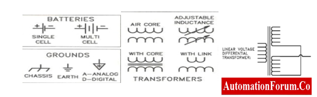
Power Sources
- The power source can be specified using a number of power source circuit symbols, just as there are numerous possibilities for powering your project.
Sources of DC or AC Voltage
- When working with electronics, constant voltage sources will be used the majority of the time.
- To indicate whether the source is supplying direct current (DC) or alternating current (AC), we can use any of these two symbols:
Batteries
- Batteries typically have the appearance of two disproportionate, parallel lines, whether they are those cylinder-shaped alkaline AA batteries or rechargeable lithium-polymer batteries.
- More pairs of lines often imply that the battery has more series cells.
- Additionally, the longer line typically connects to the positive terminal, whereas the shorter line does the opposite.
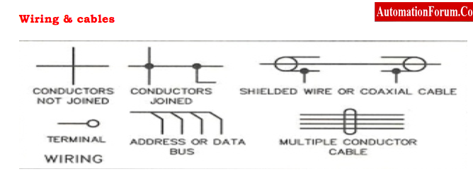
Wiring & cables
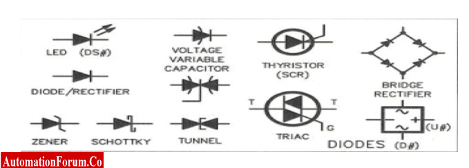
Diodes
- Generally, a triangle pressed up against a line is used to represent basic diodes.
- Due to the polarisation of diodes, each of the two terminals needs distinguishing labels.
- The terminal sloping into the triangle’s flat edge is the positive anode.
- In the symbol, the negative cathode protrudes beyond the line (think of it as a – sign).
- There are many distinct kinds of diodes, and each one has its own unique variation on the basic diode symbol.
- Light-emitting diodes (LEDs) add a few lines pointing away to the diode symbol.
- The arrows are turned around and pointed in the direction of the diode by photodiodes, which are essentially small solar cells that produce energy from light.
- With modest modifications to the bar portion of the sign, other specific types of diodes, such as Schottky’s or zeners, have their own symbols.
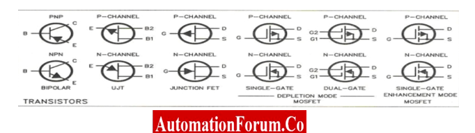
Transistors
Transistors—BJTs and MOSFETs—can be positively or negatively doped.
There are two ways to draw each transistor type.
BJT’s
- BJTs have a base, collector, and emitter (B). NPN and PNP BJTs have different symbols.
- The collector (C) and emitter (E) pins are inline, however the emitter should always have an arrow.
- PNPs are inward-pointing, while NPNs are outward-pointing.
- “NPN: not pointing in” is a memory aid.
MOSFET’s
- MOSFETs feature three terminals—source (S), drain (D), and gate (G)—like BJTs (G).
- Again, n-channel and p-channel MOSFETs use different symbols.
- Each MOSFET type has several common symbols. The bulk (arrow) in the symbol determines whether the MOSFET is n-channel or p-channel. The arrow indicates n- or p-channel MOSFETs.
Digital Logic Gates
- AND, OR, NOT, and XOR have distinct schematic symbols
- The shapes should remain the same (okay, maybe a little bit larger), and there should still be just one output even if they have more than two inputs.
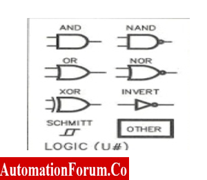
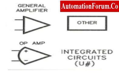
Integrated Circuits
- Integrated circuits do so many unique activities that they don’t need a separate circuit symbol. Integrated circuits are rectangles with pins.
- Pins should have numbers and functions.
- IC names, values, and labels matter because of their generic circuit symbol. Each IC should have an exact chip name value.
- Some typical integrated circuits have a distinctive circuit symbol with five terminals: a non-inverting input (+), inverting input (-), output, and two power inputs.
- Three-terminal voltage regulators typically have input, output, and ground (or adjust) pins.
- These rectangles have pins on the left (input), right (output), and bottom (ground/adjust).
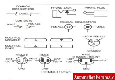
Connectors
- Electrical and electronic connectors are essential parts of all designs because they are used to join wires and cables in electrical and electronic circuits.
- Jacks and plugs (male-ended) make up connectors (female-ended).
- The connection may be used as a temporary electrical joining between two wires or devices, as with portable equipment, need a tool for assembly and removal, or be a permanent electrical joint.
Tubes and Tube elements
- The confusion is minimized if a specific tube is represented by a tube symbol.
- Today’s circuits use a lot of tubes with internal connections between their component parts.
- Similar to other tubes, only specific parts of them are actually connected to circuit components.
- When drawing schematics, these elements cannot be disregarded.

Miscellaneous representation

Nets, Nodes and Labels
- Schematic nets explain how circuit components are connected to one another. Between component terminals, nets are shown as lines. In this schematic, the green lines are an example of when (but not usually) they have a special color.
Junction Node

- Wires can join two terminals together or dozens of terminals.
- A junction is made when a wire breaks into two directions.
- Nodes, which are tiny dots positioned at the wire intersections, are used to depict junctions on schematics.

Net Names
- Instead of distributing a wire throughout the schematic, we will occasionally name and label a net to make diagrams easier to read.
- Names may be written directly on the net or may be attached to “tags” that hang from the wire.
Electronic symbols of Solid state devices, Switches, Fuses, Meter
Electronic schematics
- Schematic diagrams are used to display the placement of components on a circuit board as well as the connections between them.
- It should be remembered that a schematic diagram cannot tell you where a component is actually located on a circuit board.
- The schematic depicts the components and connections but not their precise positions.
- They are the hardest drawings to interpret because they require a deep understanding of how each electronic component affects or is influenced by an electrical current.
- Schematics guide circuit planning, construction, and troubleshooting.
- Schematic reading is essential for electronics engineers.
- Electronic schematics are the most complex. They depict each circuit component, its ratings, and its wiring.
- Block diagrams are the simplest. Block diagrams are simple geometric shapes that depict any element, component, or system.
- Each block may represent a relay, a collection of components, or a system. The drawing’s purpose determines each block’s detail.
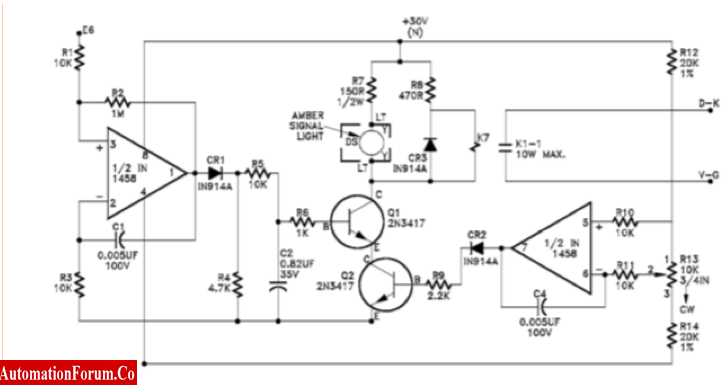
Examples of Electronic Schematic Diagrams
- There is a symbol for every single part of an electronic circuit in an electronic schematic.
- The diagrams only depict the system’s functionality and movement, not its location or size.
- The inner workings of a certain electronic device can be deduced from this.
- You may see an example of a schematic diagram below that shows how electronics work.

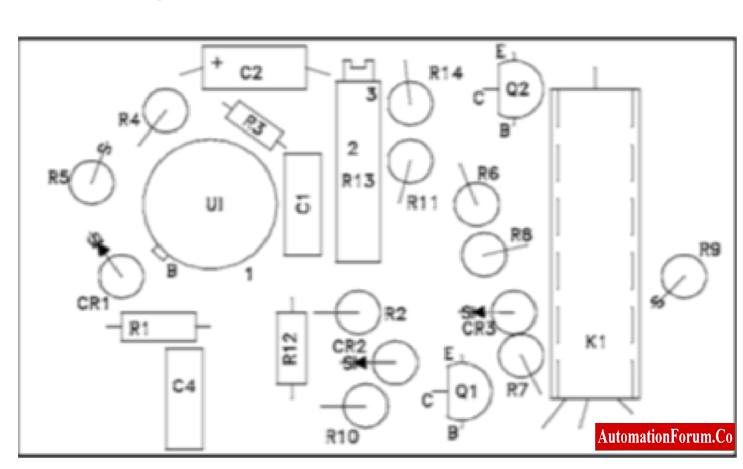
- The visual layout diagram, a different kind of electronic schematic, is more like a picture of how the actual electronic circuit appears than a true electronic schematic.
- The actual placement of the components on the circuit board is depicted in these drawings.
- This is a two-dimensional drawing that details the components in their location and is often viewed from the top looking down.
- Compares a circuit’s schematic with a layout or graphical representation of the same circuit.
- Typically, a parts list would be included with the visual layout.
Reading electronic prints or schematics
- The markings are used to indicate bistable operation when examining electrical prints or schematics.
- Bistables are typically denoted by a box or circle, as shown below. These bistables are identified by the lines inside or around them, which also show how they work.

- The several conventions used to denote bistable operation are shown in Figure(B). One circuit will frequently connect with another, thus it’s important to have a mechanism that enables the reader to trace a single wire or signal channel from one picture to the next.
- There are numerous ways to accomplish this, but often the line or conductor that needs to be continued ends at a terminal board.
- The continuation drawing will be noted on this board, which will be numbered and labeled (a separate drawing may exist for each line).
- The terminal board that corresponds to the prior number can now be discovered and the next drawing can begin.
- The conductor should conclude with a number (often a single digit) and the next drawing number when terminal boards are not being used.
- On some drawings, coordinates are given that show where the continuation is located on the second drawing, making it easier to find the continuation.
- The second drawing’s continuation point will also refer to the previous drawing’s continuation coordinates.
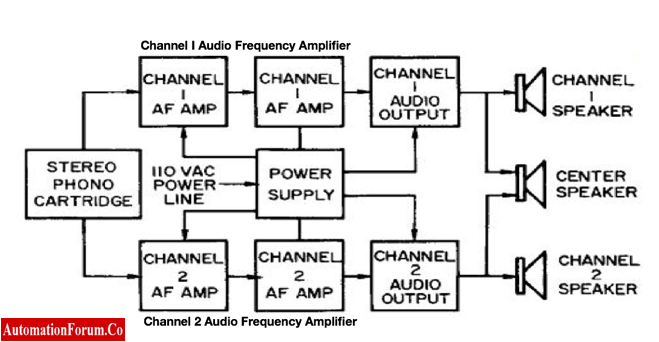
Block Diagram
- The most fundamental and straight forward engineering print type is the block diagram. It is made up of basic building pieces that can be used to represent any quantity.
- Each block represents a signal step that is displayed on the bottom meter or routed to systems outside the illustration.
- Some have many functions, while others are basic stages or bi-stable circuits in bigger components.
- The block diagram’s creator chooses each block’s content based on its use.
- Many times, two or more different styles of drawings will be integrated into a single print.
- This makes it possible to deliver the relevant data in an organized and understandable manner.
- Since block diagrams are frequently used with sophisticated schematic diagrams to help illustrate or summarize their flow or functional information, block diagrams are shown with electronic schematics in this section.
- Block diagrams offer a way to graphically represent any kind of electronic circuit or system.
- Block diagrams are not intended to display precise component information, but rather flow or functional information about the circuit or system.
Block Drawing Symbology
- Block diagrams employ the symbols in below figure as a starting point.

- The fundamental building components depicted above figure can be utilized for just about anything when block diagrams are applied.
- The block will have whatever is typed inside it.
- Block diagrams are not only used in electronic circuits.
- Block diagrams are frequently used to depict intricate instrument channels and other intricate systems when only the signal’s flowpath is crucial.
Examples of Block Diagrams
- Diagram following is an example of block diagram.
- An instrumentation channel that measures neutron flux, displays the measured flux, and produces output signals for use by other systems is shown in this block diagram. Block diagrams are not only used in electronic circuits.

Second example of block diagram.
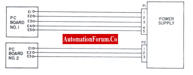
Connection Diagrams
- Connection diagrams are used to demonstrate the interconnections between the parts of an electronic system.
- They serve as a guide for putting together and managing electronic systems.
Four different types of connection diagrams exist:
- Point-to point diagrams
- Baseline diagrams
- Highway diagrams
- Lineless diagrams
Point to Point Diagram
- This particular style of connection diagram displays the numerous terminal connection points and the wires’ exact routing pathways.
- With basic circuits, point-to-point schematics are primarily used.
Steps involved in creating point to point diagram
- Sketch each electronic component in the circuit in its proper location.
- Draw the course of the wire.
- Indicate the wire colors.
Baseline Drawing
- Every wire path enters a single baseline.
- They are simpler to read and understand than point-to-point diagrams, but because they do not display the electronic components in their correct places, they can be deceptive.
Steps involved in creating baseline diagram
- Create the baseline by drawing a thick line.
- Draw the electronic parts, placing half above and half below the baseline.
- Sketch lines connecting each connection point to the baseline. The line has to run parallel to the baseline.
- Add a destination code to each wire path.

Highway Diagram
- This kind of wiring schematic puts together wires that follow similar routes into units known as “highways.”
- Highway diagrams are similar to point-to-point diagrams in that the components are situated where they would be found in the actual circuit.
Steps involved in creating highway diagram
- Sketch the electronic parts in their correct locations.
- Draw a rough outline of the wire pathways to identify suitable highway locations.
- Dim the components, connection points, and lines leading to the highways.
- Label the wire pathways with the component number, wire color, and destination code.

Lineless Diagram
- This particular style of connection diagram labels the connecting locations on the electronic components but does not display any cables.
- The components come with a table that lists the designation, color, and destination code for each wire in place of wires.
Steps involved in creating line-less diagram
- Sketch the electronic parts in roughly the areas where they will be held in the actual circuit.
- Put the wiring table together.

Rules for drawing Schematic
The rules are as follows:
- Inputs go to the left
- Outputs go to the right
- Connectors should be broken and pins should be jumbled
- Ground should be pointing downward
- Curved sides of capacitors should be pointing to ground
- Crossovers should be avoided, and components shouldn’t be crammed together.
- The signs were numbered from left to right and top to bottom.
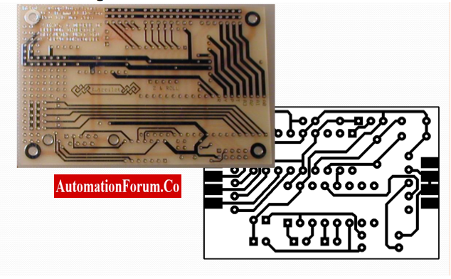
Example of Connection Diagrams with PCB

PCB-Component Diagram

PCB Circuit Diagram