What is meant by Latches in digital electronics?
Latches is defined as a logical circuit that is used for storing single binary digit. Latch stores data using a feedback loop that helps memory elements to store binary information.
The feedback loops are created in circuit diagrams so that output values depend on themselves indirectly.
Input of a latch works as an electronic switch to control the state of device. Latch circuits have two output stable states, LOW & HIGH.
Therefore, latch is also called as bistable-multivibrator. A latch’s output depends on its current and previous inputs, and its state can change at any time when input changes.
What are latches used for?
As Latches store data, it is used as memory elements. Latches are used in building flip-flop which is used for designing a sequential logical circuits.
What are the types of latches?
The types of latches are classified as
- SR Latch
- Gated S-R Latch
- D latch
- Gated D Latch
- JK Latch
- T Latch.
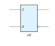
SR Latch
What is meant by SR Latch?
S stands for set and R stands for reset. There are two inputs S is used for set and R is used for reset. The output of SR depends on current as well as previous state. And its state changes as soon as input change.
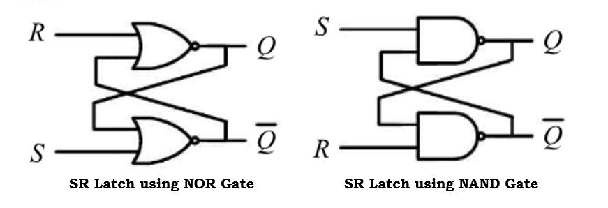
The SR latch can either be designed either using NOR gate or using NAND gates. The graphical representation of SR latch is shown below
Working of SR Latch
The working of SR Latch depends on inputs S – Set & R – Reset.
The two useful states are as follows:
If output Q = 1 and Q= 0 then latch is in set state.
If output Q = 0 and Q= 1 then latch is in reset state.
If the circuit is designed using NOR gate then for both S =R=0 then Q and Q will retains the previous state represented as Q0 which is said to be No change and S=R=1, then the output states are said to be invalid or undefined.
If circuit is designed using NAND gate then for both S =R=1 and S=R=0, then the output states will be reverse of the NOR gate.
Circuit Diagram of SR Latch
Truth Table of SR Latch
| S | R | Q | State |
| 0 | 0 | Q0 | No Change |
| 0 | 1 | 0 | Reset |
| 1 | 0 | 1 | Set |
| 1 | 1 | Q = Q = Invalid | |
Gated SR Latch
What is meant by Gated SR latch?
A modified SR latch called a “Gated SR Latch”. It has three inputs which are Set, Reset, and Control/Enable. The SET and RESET inputs are only functional when the controlling input is switched on. The SET and RESET inputs of a gated SR Latch are operable when the control input is enabled. A switch is used to connect to this control input. When the control is 1, the Set-Reset inputs are activated. When the control is 0, the Set-Reset inputs are disabled, the output retains in previous state.
The Gated SR latch’s graphical diagram with circuit diagram and truth table are shown below.

Circuit Diagram of Gated SR Latch:

Truth table of Gated SR latch:
| Control(C) | S | R | Q | State |
| 0 | x | x | Q0 | No change |
| 1 | 0 | 0 | Q0 | Nochange |
| 1 | 0 | 1 | 0 | Reset |
| 1 | 1 | 0 | 1 | Set |
| 1 | 1 | 1 | Q = Q = Invalid | |
D Latch
What is meant by D Latch?
In SR Latch, when S and R are both 1, we obtained invalid state where we cannot determine the next state value. This can be modified by using D latch. The D latch is also called as Data Latch or Delay or Transparent latch.
In simple D latch circuit diagram is obtained by modified SR Latch circuit diagram.
Circuit Diagram of D Latch

Working of D Latch
D latch circuit has one input D and 2 outputs Q &. By inserting an inverter between the S and R inputs and connecting the D input to the S, a D latch is created from an SR latch.That means we eliminated the combinations of S & R of same value.
- If D = 0 then S = 0 & R = 1, output Q will be equal to ‘0’ irrespective of present state Q0, which is shown state table.
- If D = 1 then S = 1 & R = 0, the output Qwill be equal to ‘1’ irrespective of present state Q0which is shown in third row of D Latch following table.
Truth Table of D Latch
| D | Qo | Q | |
| 0 | X | 0 | 1 |
| 1 | x | 1 | 0 |
Gated D Latch
What is meant by Gated D Latch?
The Gated D Latch has 2 inputs – Data, Control. The output is identical to Data input when control input is set to 1. Because of this reason the D latch is also called as Transparent Latch. If Control input is 0 the output is unchanged.
Gated D latch is designed by modifying gated SR latch. The set and reset inputs are connected via an inverter. If this is done, the output will be opposite to one another. The Gated D latch’s graphical diagram with circuit diagram & truth table is shown below.

Circuit Diagram of D Latch

Truth Table of Gated D Latch
| C | D | Q | Q |
| 0 | x | No change | |
| 1 | 0 | 0 | Reset State |
| 1 | 1 | 1 | Set State |
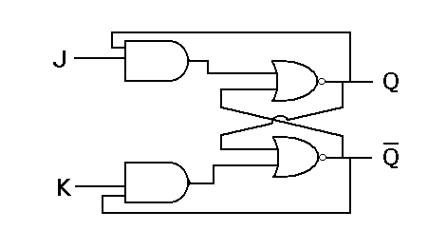
JK Latch
What is meant by JK Latch?
The SR Latch and the JK Latch are identical. When the JK inputs are high, the unclear states are eliminated in a JK latch, and the output is toggled.
The main distinction between SR latches and JK latches is that SR latches lack output feedback toward the inputs while JK latches have.
The circuit diagram and truth table of the JK latch are shown below
Circuit Diagram & Truth table of JK Latch
| J | K | Q | State |
| 0 | 0 | Q | No Change |
| 0 | 1 | 0 | Reset |
| 1 | 0 | 1 | Set |
| 1 | 1 | Q | Toggle |
T Latch
What is meant by T Latch?
The JK latch inputs are shorted to create the T latch. The T latch’s output switches on and off when the input is set to 1 or high.When the input of T is 0 then the output will retain the same (no change). The circuit diagram and truth table of the T latch is shown below.
Circuit Diagram & Truth Table of T Latch

| T | Output |
| 0 | No Change |
| 1 | Toggle |
ADVANTAGES AND DISADVANTAGES OF LATCHES
Advantages of the latches
- Latch designs made using logic gates take up less area.
- Because the latches don’t behave sequentially, they steal the cycle when it’s necessary to finish the task.
- These are renowned for being rapid by nature and for responding to inputs.
- It consumes less energy.
Disadvantages of latches.
- Race-around and toggling scenarios are present in the circuit as a result of the bits’ desertion.
- Latch analysis in the circuit becomes difficult because of level sensitivity.
Applications of Latch
- It is well known that these circuits may store information as bits. Memory elements are those things.
- The use of pulse latches produces a rapid reaction while yet mimicking flip-flop behavior.
- Data latches (D-Latches) are employed in two-phase synchronous systems to prevent the transit count.
- It is frequently used to store data and computation codes.