- What is a Transistor?
- Layers of a Transistor
- Parts of a Transistor
- Types of Transistors
- Working Principle of Transistor
- How Do Transistors Work?
- Making of transistor
- Characteristics of a Transistor
- Limitations of Transistors
- Applications of Transistors
- Frequently Asked Questions on Transistors
- Which region of the transistor is lightly doped?
- How is the emitter region of the transistor different from the collector region?
- What is the normal biasing of the diodes in a transistor?
- How many depletion regions does a transistor have?
What is a Transistor?
The transistor is an active component and a semiconductor device that is used as an amplifier to amplify the high- and low-level signals and utilized in oscillators, detectors, modulators as well as it can be employed as an electrically controlled switch in digital circuits. So, in simple words, it can be said that a transistor is a miniature form of a device that can be used to regulate or restrict the flow of electronic signals.
Transistor has become the most important element in modern electronics. Transistor was developed in the year of 1947 by three American physicists, named Walter Brattain, John Bardeen, and William Shockley.
Layers of a Transistor
A transistor is comprised of three layers of semiconductor materials, typically terminals. These terminals help to make a connection with an external circuit and flow of the electric current. The current through the transistor in a pair of terminals is controlled by the voltage or current applied to the other pair of terminals. The three layers of the transistor are mentioned below:

Base: This terminal is used to activate a transistor
Collector: This layer is called the positive lead of a transistor
Emitter: This is the negative lead of a transistor
Parts of a Transistor
A transistor typically consists of three layers of semiconductor material, forming terminals that connect to an external circuit and facilitate current flow. By applying a voltage or current to one pair of terminals, the current through the other pair is controlled. The three terminals of a transistor are as follows:
Emitter: Functions as the negative terminal that releases the current.
Base: Serves as the control terminal that activates the transistor.
Collector: Acts as the positive terminal where the current enters.
Types of Transistors
There are various types of transistors and they are classified based on their structure. Each type of transistor has its own characteristics and different application. On a broader scale, the transistor is classified in the below categories

Transistors are majorly classified into two broad categories: BJT and FET
Bipolar Junction Transistor (BJT)
- BJTs are basically composed of three terminals, the base, the collector, and the emitter. In this device, ‘Bipolar’ means both electrons and holes which are essentially required for current flow and the term ‘Junction’ means PN junction. BJTs are basically current-controlled devices. If a little amount of current is applied to the base of a BJT transistor, a large amount of current flows from the emitter terminal to the collector. These transistors are basically operated in three regions:
- Cut-off Region: In this region, no current flows through the transistor and the transistor acts as an open switch. Here the transistor stays in an ’OFF’ state.
- Active Region: In this region, the transistor operates as an amplifier.
- Saturation Region: Transistor acts as a closed switch in this mode of operation and it remains in a fully ‘ON’ state.
BJTs are classified into two major categories:
PNP Transistor
This is one kind of Bipolar Junction Transistors – BJT and it comprises two p-types of semiconductor layers. These materials are separated by a lean layer of n-type semiconductors. In this type of transistor, holes are the majority charge carriers and the minority carriers are the electrons.
PNP transistor is in, active or ON state when the current at the base terminal is kept low with respect to that of the emitter. Hence, in the PNP transistor, the base is always negative with respect to the emitter and collector terminals. The current that enters the base is amplified before reaching the collector terminal. The emitter-base junction is forward biased as the collector-base junction is reversed biased.
The PNP transistor is denoted as ‘PNP’ and the diagram below is the symbol of the PNP transistor. The conventional current flow is indicated by the arrow symbol and the current will be directed from the emitter terminal to the collector terminal of the transistor.

Below is the structure of a PNP transistor where the forward-biased emitter pulls the electrons to the source (battery) so that the current can flow from the emitter to the collector terminal.

NPN Transistor
This is also one kind of bipolar transistor that is comprised of two n-type semiconductor materials and a p-type semiconductor is fused between the two n-type semiconductor layers in this configuration. Unlike the PNP transistor, here the majority of charge carriers are electrons and the minority carriers are holes. The flow of electrons from the emitter terminal to the collector terminal causes the current flow within the base terminal of the transistor. This is a device that is controlled by current. In the modern era, the most commonly used BJTs are NPN transistors. A negative-positive-negative transistor is symbolized by the abbreviation ‘NPN’. The below figure depicts the NPN transistor:

The standard equation for the current flowing in this transistor is:
IE = IB +IC
Construction Structure of the NPN Transistor
The construction structure of the NPN transistor is given below:

Field Effect Transistor (FET)
The Field-Effect-Transistor (FET) is another major and important classification of transistors which is a unipolar device. Like BJT it is also having three terminals. The terminals are:
Source: This is the terminal of FET through which the majority of carriers enter the bar. Hence, it is named as Source.
Drain: Through this terminal, the majority of carriers lead the bar.
Gate: These are two heavily doped terminals that are internally connected which form the PN-junctions.
FETs are broadly classified into two categories:
- JFET
- MOSFET
JFET
The abbreviation of JFET is Junction Field Effect Transistor. These are the simple and major types of transistors that are majorly used as amplifiers, switches, and resistors. JFET is a voltage-controlled device and it doesn’t require any biasing current. In this type of transistor, the flow of electric current between the source and the drain is controlled by the voltage applied between the gate and source.
JFET is of two types. Those are n-channel FET and p-type FET. In N-channel FET, to the n-type substrate, a p-type material is added. In the same manner, in the P-type FET, to the p-type substrate, an n-type material is added.
N-Channel JFET
This kind of FET is mostly used. In this type of transistor, the current flow is due to electrons. For current flow, a channel is formed between the source and drain when a voltage is applied between gate and source.
For the sake of understanding the fabrication process of N-channel JFET, a narrow bar of N-type semiconductor is considered here, and P-type material is produced on the opposite side of the bar by a diffusion process. Both the sides are joined to make a single connection through the gate terminal which is depicted in the figure below:

At the two ends of the n-type semiconductor bar, an ohmic contact is made and these form the source and the drain. Both the terminals may be interchanged. The symbolic representation of N-channel JFET is shown below:

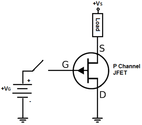
P-Channel JFET
In this kind of JFET, holes are the majority charge carriers and are responsible for current flow. It is made of a P-type silicon channel which consists of two N-type silicon terminals situated at both sides. The gate terminal is connected to the N-type material, whereas the source and drain terminals are connected to the edges of the P-type channel.
The electric current (holes) can flow freely within the central P-channel even when no voltage is applied to the gate terminal of a P-channel JFET. This is the reason why JFETs are called ‘normally ON’ devices as the current can pass across the source to drain even without any voltage.
The construction of P-channel JFET is depicted below figure:

The figure below shows the various parts of a P-channel JFET
MOSFET
MOSFET is abbreviated by Metal Oxide Semiconductor Field Effect Transistor which is very popular in the transistor family. It comprises four terminals, Source (S), Drain (D), Gate (G), and Body (B). MOSFET can be employed in both analog and digital circuits. The general construction of MOSFET is shown below in the figure.

As the Gate region of MOSFET is totally insulated from the Source-Drain region, it is often called Insulated Gate FET. In this transistor, the body or substrate is the main Semiconductor (Silicon) in which the fabrication of FET is done. The MOSFET functionality depends on the variations in electric current that occurred in the channel width as well as the flow of the charge carriers; either electrons or holes. Through the source terminal, the charge carriers enter and come out from the drain. The below figure shows the symbol of MOSFET.

Voltage is applied on an electrode called the gate which controls the width of the channel. MOSFET functions in two modes:
- Depletion Mode
- Enhancement Mode
Depletion Mode
In this mode of operation, the channel has maximum conductance when no voltage appears across the gate terminal, whereas when the voltage is either positive or negative across the gate, the conductivity in the channel decreases.
Enhancement Mode
No conductivity is present when there is no voltage across the gate terminal. When the voltage across the gate is at its maximum, the conductivity of the device is enhanced.
Depletion and Enhancement types are also available in two types; N-channel and P-channel types.
N-channel MOSFET
In this type of MOSFET, N-channel is present between source and drain. Here, the source and drain terminals are doped heavily by n-type material which is placed in the p-type semiconductor layer, or substrate which is heavily doped.
Here, electrons are only responsible for the current flow between the source and drain zone and the current flow is typically controlled by the gate voltage. The below figure depicts the symbol of N-channel MOSFET.

P-channel MOSFET
Here P-channel is present between the source and drain. P-type materials are used for doping the source and drain terminals, whereas the N-type materials are used for doping the substrate. Here, holes are the majority carriers that cause the flow of current and the current flow is controlled by the voltage applied across the gate terminal.
The symbol of P-channel MOSFET is shown below:

Working Principle of Transistor
There are various types of transistors available, but for the sake of understanding, a common emitter configuration of NPN transistor is considered here. In this type of transistor, the emitter region is wider and highly doped as the number of majority carriers (electrons) is huge here. The collector region is comparatively less doped and so here the number of electrons is not as much as in the emitter region. The base region is quite thin as is lightly doped and diffused in between emitter and collector. The number of holes (majority carriers) is quite little here.

Now, in this situation, if we connect a battery in between the emitter and collector, the emitter region will be connected to the negative terminal of the battery. Hence, the emitter-base junction is forward biased and the collector-base is reverse biased. In this mode of operation, no current flows through the transistor device. In actual practice, as the emitter region is heavily doped, the concentration of free electrons in this region is large. On the other hand, the base region is thin and there are very few holes. The collector region is comparatively wider and moderately doped.

When a voltage is applied between the emitter and collector, the entire voltage is dropped in two places; one is at the emitter-base junction at the forward barrier potential region which is about 0.7V in the case of silicon transistor and the other drop occurs at the base-collector junction at reverse barrier region. No matter what is the applied voltage, the voltage drop across the emitter-base junction always remains constant and is 0.7V, and the rest of the voltage drops across the base-collector junction. As a result, the collector voltage can never overcome the forward potential and no free electron can cross the barrier in the emitter region and come to the base region. At this condition, the transistor behaves like an off switch.

When a positive voltage is applied across the base terminal, the base-emitter junction is forward biased and now it is able to overcome the forward potential barrier and hence the electrons in the emitter region will easily cross the junction and get in touch with the base region where recombination occurs due to the presence of few numbers of holes in that place. But the free electrons which are escaping from the emitter region get some kinetic energy due to the electric field present in that junction. As the base region is thin, the electrons coming from the emitter don’t get enough time for recombination and cross the reverse-biased depletion layer and finally go to the collector zone. The free electrons in the base region are the majority carriers and hence their flow is not obstructed as a reverse barrier present in the base-collector zone. As a result, the electrons flow from the emitter to collector and collector to emitter region. There are only a few holes present in the base region with which the electrons coming from the emitter region recombine and produce a smaller amount of base current.
How Do Transistors Work?
Here’s an overview of how transistors operate:
A Bipolar Junction Transistor (BJT) has three terminals: Emitter, Base, and Collector. It is a current-driven device containing two P-N junctions:
- One junction is between the emitter and base regions.
- The other junction is between the collector and base regions.
A small current flowing from the emitter to the base can control a much larger current flowing from the emitter to the collector.
During typical BJT operation:
- The base-emitter junction is forward-biased.
- The base-collector junction is reverse-biased.
When a current passes through the base-emitter junction, it allows current to flow through the collector circuit.
For example, in an NPN transistor, electrons are the primary current carriers. The same principles apply to a PNP transistor, but the current carriers are holes, and the voltage polarities are reversed.
Making of transistor
There are two major procedures for making transistors:
Alloy Diffused Transistor
There are varieties of methods through which a transistor can be produced. In this process, a thin wafer of Germanium is used to make the base terminal of the transistor. Two pellets of Indium are diffused to either side of a wafer of the N-type base as it is a trivalent material with three electrons at its valence shell to make the collector and emitter terminals of the transistor.

Silicon Planar Transistor
Its construction is more complex compared to the alloy diffusion technique. This process requires many separate steps like depositing the oxide layers on the silicon wafer and etching away unwanted silicon areas. To shape the required patterns or layers, the steps are repeated with many variations to form a transistor or integrated interconnected circuits.

Characteristics of a Transistor
Transistor characteristics are graphical representations that illustrate the relationships between current and voltage in a transistor for a specific configuration. These characteristics are classified into three main types:
- Input Characteristics: Describe how the input current changes with variations in input voltage while keeping the output voltage constant.
- Output Characteristics: Show how the output current varies with changes in output voltage while keeping the input current constant.
- Current Transfer Characteristics: Depict the relationship between the output current and the input current while keeping the voltage constant.
Input Characteristics
CB (Common Base) Configuration:
This characteristic shows how the emitter current (I?) changes with variations in base-emitter voltage (V_BE) while maintaining a constant collector voltage (V_CB).

CC (Common Collector) Configuration:
Illustrates the variation of base current (I_B) with changes in collector-base voltage (V_CB) while keeping collector-emitter voltage (V_CE) constant.

CE (Common Emitter) Configuration:
Displays the relationship between the base current (I_B) and base-emitter voltage (V_BE) while keeping collector-emitter voltage (V_CE) constant.

Output Characteristics
CB (Common Base) Configuration:
Shows how the collector current (I_C) varies with collector-base voltage (V_CB) while keeping the emitter current (I?) constant.

CC (Common Collector) Configuration:
Depicts the variation of emitter current (I?) with collector-emitter voltage (V_CE) while keeping the base current (I_B) constant.

CE (Common Emitter) Configuration:
Demonstrates the change in collector current (I_C) with variations in collector-emitter voltage (V_CE) while keeping the base current (I_B) constant.

Current Transfer Characteristics
CE (Common Emitter) Configuration:
Shows the variation of collector current (I_C) with base current (I_B) while keeping collector-emitter voltage (V_CE) constant.

CB (Common Base) Configuration:
Describes the relationship between collector current (I_C) and emitter current (I?) while maintaining a constant collector-base voltage (V_CB).

CC (Common Collector) Configuration:
Displays how the emitter current (I?) varies with base current (I_B) while keeping collector-emitter voltage (V_CE) constant.

Advantages of Transistors
- Transistors are inexpensive to manufacture and occupy minimal space, making them ideal for small and cost-sensitive electronic devices.
- Unlike vacuum tubes, transistors have no moving parts, making them less prone to mechanical failures and more robust in various applications.
- Transistors function efficiently at low voltages, making them suitable for battery-powered and low-energy devices.
- Due to their solid-state nature and lack of filaments or fragile components, transistors have a much longer operational life compared to older technologies like vacuum tubes.
- When in an off state, transistors consume virtually no power, making them highly energy-efficient components in digital circuits.
- Transistors can switch on and off very quickly, enabling their use in high-speed computing and communication systems.
- Transistors allow for the design of highly efficient electronic circuits, minimizing energy loss and heat production.
- Transistors are foundational in creating integrated circuits, which combine thousands or millions of transistors in a single chip for complex operations.
Limitations of Transistors
- Exposure to cosmic rays and radiation can alter transistor functionality, especially in aerospace and nuclear environments, requiring radiation-hardened designs for such applications.
- Compared to certain alternatives like vacuum tubes in high-frequency applications, transistors exhibit lower electron mobility, which can limit their performance in some cases.
- Transistors can be easily damaged by events such as power surges, overheating, or electrostatic discharge during handling, necessitating careful design and precautions.
Applications of Transistors
- Transistors operate as a switch in digital and analog circuits or both for switching and amplification purpose. Our cell phone uses the transistor amplifier which is a widely used application.
- Used for signal amplification
- Used in the power supply part as a power amplifier in the devices like AC to DC adapters, Mobile phone chargers, SMPS, Tape recorders, Power supply section of TV, etc.
- Transistors are employed to build various integrated circuits like Microprocessors, Microcontrollers, Logical blocks, etc. and the logical operations in microcontrollers are done using transistors. In each chip of a microprocessor, it requires a billion transistors.
- Used in almost every electronic device starting from computers to aircraft.
- Transistor’s high power radio frequency (RF) is often used in radar or hand-held two-way radios.
- Darlington pairs of transistors are sometimes used in light-sensing and touch-sensing devices.
Frequently Asked Questions on Transistors
Which region of the transistor is lightly doped?
The base region of the transistor is lightly doped to ensure proper control over the current flow between the emitter and the collector.
How is the emitter region of the transistor different from the collector region?
The emitter is more heavily doped than the collector. This allows the emitter to inject a large number of charge carriers into the base, while the collector, being larger and less doped, collects these carriers efficiently.
What is the normal biasing of the diodes in a transistor?
In normal operation:
- The emitter-base junction is forward-biased.
- The collector-base junction is reverse-biased.
This configuration enables the transistor to amplify signals or act as a switch.
How many depletion regions does a transistor have?
A transistor has two depletion regions, one at each P-N junction:
- Between the collector and base.
- Between the emitter and base.