- Transistor
- What are the types of transistor?
- What are the types of BJT and symbol?
- What are the types of Packages?
- How to identify transistor terminal leads?
- Explain about the different types of transistor package
- Transistor Outline Package
- How to identify the terminals in transistors Family
- Field Effect Transistor(FET)
- MOSFET – Metal Oxide Semiconductor Field Effect Transistor
- IGBT- Insulated Gate Bipolar Transistor
- Special Purpose Transistor
- Phototransistor
- UJT – Unijunction Transistor
Transistor
What are the types of transistor?
- BJT stands for Bipolar Junction transistor – Current controlled device
- FET stands for Field Effect Transistor – Voltage controlled device
- IGBT stands for Insulted Gate Bipolar Transistor – Voltage driven device
- Special Purpose Transistor – Phototransistor & Unijunction Transistor
What are the types of BJT and symbol?
- NPN Transistor
- PNP Transistor
They are three terminal devices. The terminals in transistor are
- Base (B)
- Emitter (E)
- Collector (C)

What are the types of Packages?
- Small-Outline Transistor (SOT)
- Transistor outline (TO)
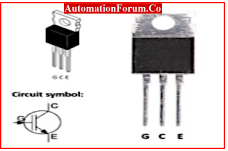
How to identify transistor terminal leads?
- NPN or PNP transistors are available in plastic or metal can packaging and can be either NPN or PNP.
- The transistor’s front side is flat when it is enclosed in a plastic case, and the pins are arranged serially.
- Keep the front flat side of the pins facing you while you count the pins as 1, 2, etc. to identify them.
- It will typically be first is Collector, second pin is Base and last is Emitter. Therefore, CBE.
- In contrast, the situation will simply be reversed in PNP transistors. EBC is that.

Explain about the different types of transistor package
Transistor components are housed in special cases known as transistor packages that connect the internal and external circuits, protect the sensitive internal components, and may even have the ability to dissipate heat using heatsinks to prevent thermal damage.
According to their intended use, transistor packages vary; for example, high power transistor packaging differs from low power transistor packaging. While metal packaging for low power transistors has a protrusion (tag) on the plate beneath it, plastic packaging has a flat characteristic surface.
Higher power transistors are typically made of metal, plastic packaging, or a combination of both.Metal tags in body transistors are beneficial for attaching a heat sink or appliance exhaust heat dissipation that happens during the process. Metal tags in body transistors often indicate a collector terminal and are specialised in high power transistors.
For surface mount devices, other standards occasionally use “SOT” (small-outline transistor), while “TO” (transistor outline) is the norm for transistor packages.
Transistor Outline Package
The architecture of TO packages range greatly, from expensive plastic-moulded package bodies to metal can enclosures. The following TO-3, TO-18,TO-92, TO-220, TO-267 etc… packages are among the many available for transistors.
TO-92 transistor type package
- A little kind of plastic-moulded packaging is the TO-92.
- It has a semi-circular rear and a flat front face that is marked with the device name or number.
- The TO-92 typically has three leads, all of which emerge from the bottom of the package, as this is the configuration that is most frequently used for transistor packing.
- The TO-92 package’s primary benefit is its compact size.
- Sadly, due to its diminutive size, it cannot be utilised with devices that consume a lot of power and is not intended to remove much heat.
TO-18 transistor type package
- In To-18 is a sort of “metal can” (sometimes called a “metal header”) package for semiconductor devices.
- It is hermetically sealed to shield the technology from pollutants and moisture in the environment.
- The TO-18 resembles the TO-46 in appearance, but because to the taller cap, it is slightly larger than the latter.
TO-220 transistor type package
- TO-220 has the metal tab on the back which is used as a heat sink by itself, it contains a hole so that, in the event that more power handling capacity is needed, it can be screwed onto a bigger heat sink.
- Common transistors that are packaged in the TO-220 design.
- Devices using semiconductors and running at less than a few hundred volts and 100 amperes often have a TO-220 casing.
- The TO-220 package is not designed for electronics operating at radio frequencies since these devices operate at DC or rather low (audio) frequencies.
- Transistors that are bipolar, bipolar Darlington, and have power MOSFETs are also used.
TO-3 transistor type package
- Power transistors, SCRs, and other high-power semiconductor devices frequently employ the TO-3 or TO3 package type, a high-power dissipation device.
- The microchip is put on the metal can base of the TO-3, which is entirely constructed of metal, and is then protected by a metal cap.
- Large heat sinks can fit inside TO-3 packages, which increases their capacity for handling electricity.
- The base and emitter of a typical power transistor housed in a TO-3 package have two protruding terminals, and the collector uses the TO-3’s body as its terminal for direct thermal conduction to the heat sink.
- The benefits of the TO-3 package are – Superior durability, simple mounting, excellent power handling capacity, and hermetic sealing that shields the chip from outside influences.
SOT type package
- Surface-mount, plastic-moulded Small Outline Transistor (SOT) packages are incredibly tiny and have leads on both of their long sides.
- SOTs are commonly employed in consumer electronics due to their low profile.
How to identify the terminals in transistors Family
Field Effect Transistor(FET)
FET is classified as JFET & MOSFET which is three terminal devices. The terminals in transistor are
- Gate (G)
- Drain (D)
- Source (S)

FET Terminals Identification
- In order to recognise a Field Effect Transistor, one must turn the component so that the curved portion is facing them and then begin counting in the anticlockwise manner.
- The first one is the source, then the second one is the gate, and the third one is the drain.
- To identify a Field Effect Transistor, hold the curved portion facing them and start counting in the anti-clockwise direction. The first one is the source, next the gate and then the drain.

MOSFET – Metal Oxide Semiconductor Field Effect Transistor
The symbolic representation of MOSFET with different types is shown below.

- In most cases, the pins of a MOSFET will be appropriately labelled as G, S, and D, which stands for Gate, Source, and Drain respectively.
- In some circumstances, it is strongly suggested that the datasheet of the MOSFET be consulted.
- The pins are usually oriented so that the flat side is facing you, and they are labelled with the letters S, G, and D in order from left to right..

IGBT- Insulated Gate Bipolar Transistor
- A few useful IGBTs, like the GN2470, have raised up surfaces that are positioned so that the shorter one in the centre is the cathode and is facing the person holding the device.
- The terminal in IGBT are Gate, Collector & Emitter
- The Gate is the object on the left, while the Emitter is the object on the right.
Special Purpose Transistor
The Special design transistors arePhototransistor & Unijunction Transistor
Phototransistor
- Phototransistor as its name indicates it depends on light intensity.
- A light-sensitive region replaces the base terminal in this simple transistor.
- Hence, it has only two terminals and three terminals.
- Two terminals are used as Collector and emitter. The short pin indicates the emitter terminal
- The photosensitive region turns the light energy into electrical energy that is employed for controlling the output current.
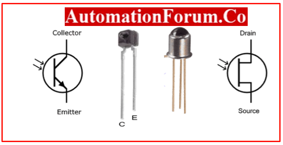
- BJT or FET can be used to make them. The BJT photo transistor converts the light energy into the base current while the FET photo transistor converts light into voltage to control the large current. When shaded or without light, it turns off.
- Light on its junction produces the base current or gate voltage proportional to light intensity, turning it on.
- It controls huge collector or drain current.
UJT – Unijunction Transistor
- UJT is device mainly used for triggering circuit, timing circuit& waveform generator. The pin arrangement is identical to a bipolar junction transistor’s.
- The terminals are Emitter, Base 1 & Base 2 as shown.
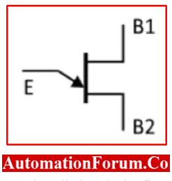
- Typically, the device is handled with the flat side facing the user.
- In order from left to right, the pins are numbered from 1 to 3.
- UJTs, such as the 2N2646, should be held with the pins facing downward. Starting clockwise, the first terminal is the Base1 terminal, the second or middle terminal is the Emitter terminal, and the third terminal is the Base2 terminal. UJT pin 2N4871 & 2N2646 is shown below.
