- What are P Type & N type material?
- What is PN Junction?
- Energy band diagram of p type & n type
- Formation of P-N Junction
- Energy level diagram for the p-n junction under thermal equilibrium condition
- PN junction energy band diagram with bias condition
- Depletion Region
- How can we refer down hill & up hill in PN junction?
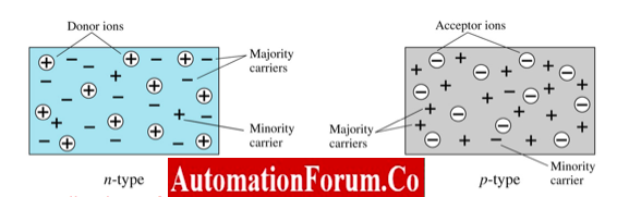
What are P Type & N type material?
- P type – Holes are majority carrier and Electrons are minority Carrier
- N Type – Electrons are majority carrier and Hole are minority Carrier
Applications of PN junction
Photodiodes, Light-sensitive diodes, LEDs, and Varactor diodes, which have variable capacitance.
What is PN Junction?
- The fundamental building block of all semiconductor devices is the p-n junction.
- Its primary electrical characteristic is that it allows current to flow easily in one direction only.
- The p-n junction is frequently referred to as a Diode.

Energy band diagram of p type & n type
- The essential characteristic of the energy band is the stability of the electronic electron’s energy states over a wide range.
- As a result, both the atom’s valence and conduction bands will have different levels of energy.

Valence Band & Conduction Band
- The valence band is the uppermost nearly filled band, whereas the conduction band is the lowermost almost empty band. The band gap is the distance between them.
Fermi Level
- The Fermi Level is the maximum energy level an electron may occupy when it is at absolute zero temperature
- Since the electrons are all in the lowest energy state at absolute zero, the Fermi level is located between the valence band and conduction band.
- There is a big discontinuity in the fermi level across the pn junction.
Ec – representation of the bottom edge of conduction band
Ev – representation of top edge of valance band
Eg – Difference between conduction band & Valence band Ec-Ev
EI– Intrinsic energy level
Formation of P-N Junction
N-type and P-type doped Silicon (or Germanium) is joined together to form a p-n junction
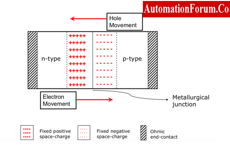
- Lots of holes want to move to the left and lots of electrons want to diffuse to the right on the junction’s right and left sides, respectively.
- Because they are elements (like arsenic and boron) that are incorporated into the lattice, the donors and acceptors are fixed and don’t move (until you heat semiconductors, so they can disperse), but the electrons and holes that originate from them are free to travel.
Ideal p-n junction
- Holes diffuses into the left of the metallurgical junction, and join with the electrons there. They leave behind acceptor regions that are negatively charged.
- Similarly, positively charged donor centers are left behind when electrons diffuse to the right.
- This diffusion process must eventually come to an end.
- Because the carriers that are attempting to diffuse away the desire to be electrostatically attracted by the growing fixed charge (donor centers want to keep the electrons and acceptor centers want to keep the holes). It achieves equilibrium.
- The diffusion process is slowed down by the electric field created by these fixed charges. It is called a depletion region because there are no more free carriers in this fixed charge region, which is also referred to as a space charge region and is where the free carriers are still present.
Energy level diagram for the p-n junction under thermal equilibrium condition
Define Drift & Diffusion current
The movement of charged particles produces current (negatively charged electrons and positively charged holes). Carrier refers to the charged electrons and holes.
In a semiconductor, there are two main mechanisms that drive electrons and holes to move:
Drift Current : Electric field-induced movement is known as drift.
Diffusion Current: Diffusion is the flow that results from changes in concentration.
Thermal equilibrium (no applied field, no net current flow)
- Since the currents are in opposition to one another, there is no net flow of current during thermal equilibrium.
- One current flow mechanism will take precedence over the other in a non-equilibrium situation, producing a net current flow.
- The potential barrier exists for the electrons that wish to diffuse from the n-type layer to the p-layer.
PN Junction Barrier height
- The built-in potential and junction potential both refer to the potential barrier height Vbi across a p-n junction.
- The potential energy of this corresponding potential barrier is qVbi.
- Electron potentials are going to be measured positively downwards since electron energy is positive upwards in the energy level diagrams.

Energy band Diagram of PN junction in thermal equilibrium

Existing mechanisms in the PN Junction in thermal Equilibrium,
- An electric in DR (Depletion Region) is caused by the carriers’ diffusion.
- Electric field in DR causes drift current to exist.
- The bulk of carriers are what cause diffusion current.
- Minority carriers are to blame for the drift current.
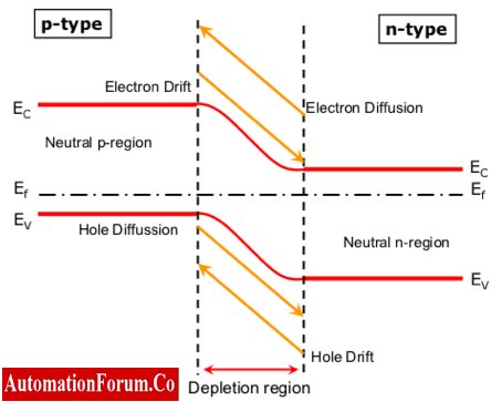
PN junction energy band diagram with bias condition
PN junction in bias condition means applying voltage. The behavior of energy bands with zero bias, forward applied voltage, reverse applied voltage are shown below.


At equilibrium
- The fermi levels on the two sides of a p-n junction match when it is in balance.
- At the junction, electrons and holes achieve equilibrium and form a depletion area.
- The diagram’s upward arrow denotes an increase in electron energy.
- That suggests that you would need to provide energy to make an electron move up the diagram and energy to have a hole move down the diagram.
At Forward Bias
- The p side is made more positive in order to forward bias the p-n junction, making it “downhill” for electron migration across the junction.
- A gap or “hole” close to the junction can be filled by an electron moving over it.
- The hole might then be said to be travelling right as it moves from vacancy to vacancy leftward towards the positive terminal.
- In the diagram, electrons conduct from right to left, and the upward trend denotes rising electron energy.
At reverse bias
- The p side of the p-n junction is made more negative to reverse-bias it, making it “uphill” for electrons to cross the junction.
- In the diagram, electrons conduct from right to left, and the upward trend denotes rising electron energy.

Depletion Region
- Depletion simply refers to a reduction in the amount of something
- Diffusion of carriers in the p-n junction area results in the depletion layer.
- The depletion region is of immobile ions because the depletion layer contains both electrons and protons, but they are immobile by nature.The potential barrier in the depletion area is caused by ions.
- Due to this depletion region in semiconductors the flow of charges slows down.
- This region serves as the barrier that prevents electrons from moving from the semiconductor’s n-side to its p-side.

How can we refer down hill & up hill in PN junction?
Down Hill – The word “downhill” refers to the way the electron flows through the PN junction under forward bias conditions where the p side is made more positive.
Up Hill – Under reverse bias condition of PN junction, the p side of the junction is made more negative which makes the electrons to cross the junction in upward direction refers to term “uphill”.