Transistor Cut-off, Saturation, Active Region
Transistor
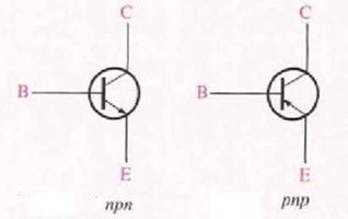
Transistor is a three-layer semiconductor device. It is consisting of either 2 N type & one P type layers of semiconductor materials or two P Type & one N type layers of semiconductor materials. This is called a NPN transistor and a PNP transistor, respectively.
Transistor is also called as BJT – Bipolar Junction Transistor. The transistor symbol for NPN and PNP is shown below.
Transistor has three terminals Base, Emitter & collector. Construction of transistor for both NPN & PNP is shown below in figure (a). Figure (b) represents the two-diode analogy of the transistor. As it shown the transistor consists of 2 junctions namely Emitter–Base (EB) junction & Base Collector (BC) junction. Figure (c) shows the NPN & PNP terminal voltage & current.

Transistor Operation
Transistor operates in three different configurations
- Common Base Configuration
- Common Emitter Configuration
- Common Collector Configuration
The transistor has two major tasks:
- Switching
- Amplification
In Common Emitter & Common Base configuration the transistor works as Amplifier & Switch. In Common Collector the transistor works as an Voltage Follower.
Transistor Modes of Operation
There are four modes of operation in transistor. They are as follows:
- Cut-Off Mode
- Saturation Mode
- Active Mode
- Reverse Active Mode
The different modes can be obtained by providing proper biasing to the input and output junctions. Considering the common emitter configuration, the circuit diagram is as follows:
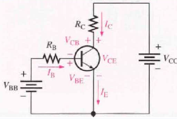
Emitters in the common emitter configuration serve as a common terminal for both input and output.
Base acts as an input terminal.
Collector acts as an output terminal.
The base terminal is biased by VBB, and the output terminal is biased by VCC.
- VBE is Input Base Emitter junction voltage.
- VCE is Output Collector Emitter junction voltage.
- IB is input Base Current.
- IC is output Collector Current.
Formula of Transistor
Then emitter current is represented as, IE = IB +IC
In Common Emitter transistor, VBE = VBB – IBRB
IC= ?IB
and VCE= ?IB + VCC
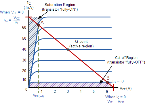
Cut-off Region of Transistor
Both the emitter base junction and the collector base junction are reversely biased in this mode. Base emitter voltage < 0.7 V (Base emitter Diode is reverse biased) therefore base emitter junction is reverse biased which means IB = 0
As we know, IC= ?IB and VCE= ICRL + VCC
In ideal case IB=0, Therefore IC= 0 & VCE = VCC
From the above expression, it is clear that transistors work as an open switch, which means the switch is in the off state. This is a shaded region near the X axis (VCE).
Saturation Region of Transistor
Both the emitter base junction and the collector base junction are forward biased in this mode. Base emitter voltage >0.7 V (base emitter diode is Forward biased) which means input junction is forward biased. Now the transistor will be biased to have the highest base current applied, therefore the collector current is high for the low collector emitter voltage drop. It is shown in the characteristics response as a shaded region near the Y axis (IC). Here with the smallest depletion layer, the highest current flows through the transistor. As a result, the transistor is turned “Fully-ON.”
As we know VCC = ICRC + VCE
When switch is fully on VCE = 0 therefore IC=VCC/RL
Also, if the emitter junction voltage is greater than the collector junction voltage, the transistor is in the forward saturation region. If the collector junction is larger than the emitter junction, the transistor is in reverse saturation.
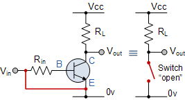
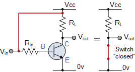
Explain transistor as Switch (SPST)
The transistor can function as a solid state “single-pole single-throw” (SPST) switch in following case
- The transistor becomes “OFF,” operating like an open switch, when a zero signal is applied to the base, and no collector current flows.
- The transistor acts as a closed switch when a positive signal is applied to its base, turning “ON” and allowing the maximum amount of circuit current to pass through the component.
Active Region of Transistor
In active mode, the input base emitter junction is forward biased and the output collector emitter junction is reverse biased. When selecting the proper operating point (Q) the transistor can be used as an amplifier. The BE junction is forward biased, so it acts as diode &therefore IB currents increase. Biasing the output junction, the collector current IC increases proportionally to the base current. The effect of output voltage VCE on the IC is negligible for the active region. Therefore IC?IB. In characteristic response, the center portion indicates the active region.
Explain transistor as an amplifier
The transistor works as an amplifier when it operates in active mode with proper biasing.
List some application of transistor when working as an amplifier:
- Fiber Optic communication
- Audio Amplification
- PA System
- Radio & TV
How Common Emitter amplifier differs from Common Base Amplifier?
Both the common emitter and common base configurations can be used as amplifiers. In Common Base, the output signal is in phase with the input signal. In common emitter configuration, the output signal is 180° from the input signal.
Reverse Active mode
This mode is the inverse of active mode. For this mode, VE should be greater than VB and VB should be greater than VC.
The emitter and collector regions interchange positions in this mode. The gain in inverted mode is much smaller because most BJTs are made to optimize current gain in forward-active mode. This mode is rarely employed. This transistor mode is taken into account for fail-safe situations and some kinds of bipolar logic. In this region, the reverse bias breakdown voltage to the base might be orders of magnitude lower. Therefore, IC is proportional to IB but the flow of current is in reverse.
Different Modes of operation of transistor
| Modes | Emitter Base (EB) Junction | Collector Base (CB) Junction | Application |
| Cut-off | Reverse | Reverse | In digital circuit as Switch (On & Off) |
| Saturation | Forward | Forward | |
| Active | Forward | Reverse | Amplifier |
| Reverse-Active | Reverse | Forward | Performance Degradation |

The above quadrant shows different mode of operation with respect to the applied voltage.
Key Questions related to Transistor Modes
What is the value of IC when transistor is said to be in cut-off region?
Transistor in cut off region means the switch is in off state. When the switch is off, the current in the circuit is zero.
How do you know if a Transistor is saturated or active?
When both collector-base & base-emitter junction is reverse biased, it is the active region and when both collector-base & base-emitter junction is forward biased, it is the saturation.
What is the difference between a cut-off region and a saturation region?
| Parameter | Cut-off Region | Saturation region |
| Junctions | Both junctions are reverse biased | Both junctions are forward biased |
| State of Device | It is fully off state, also known as open circuit | It is fully on state, also known as short circuit |
| Output Current & Voltage | Input current is zero, leads to IC =0 & VCE=VCC | Input current is maximum, leads to maximum output IC & VCE= 0 |